Technologies
RF GaN
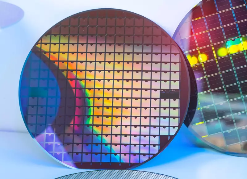
Powering the revolution of wireless connectivity with RF GaN
The number of connected devices is growing and data traffic is accelerating. Wide-bandgap materials such as gallium nitride (GaN) enable higher RF power, efficiency and frequency operation across demanding applications. Our RF GaN technologies are uniquely positioned to translate GaN’s intrinsic advantages into commercially viable solutions and overcome the limitations of existing infrastructure.

-
GaN-on-Si advantage
We uniquely leverage GaN-on-silicon (GaN-on-Si) integration to unlock GaN’s commercial potential- enabling cost-effective, high-volume manufacturing.
-
High RF performance
Excellent gain and efficiency across FR1 and FR3 frequency bands enables high-performance, power-optimized solutions for both D-mode and E-mode devices.
-
High power density
Our RF GaN offers superior performance RF for both D-mode and E-mode devices, empowering designers to optimize output power, efficiency and linearity.
-
Thermal reliability
Engineered to address thermal performance challenges inherent in high-power RF operation, supporting sustained performance in demanding applications.
-
Trusted U.S. manufacturing
Home to industry-leading RF-SOI and SiGe technologies, our accredited Burlington, Vermont facility offers time-tested robust process controls and advanced copper backend integration.
-
Backed by proven RF leadership
Building on our decades of RF expertise, our RF GaN technology offers robust PDKs with RF models, GlobalShuttle™ MPW program runs and dedicated tapeouts.


The ultimate in power density & efficiency
Harnessing GaN’s high electron mobility, low capacitance and wide-bandgap capabilities, we deliver powerful, efficient RF solutions in smaller form factors, optimized for power amplifiers, SATCOM systems and broad frequency RF applications.
-
Excellent gain in FR1 & FR3 frequency bands
High RF power density with exceptional efficiency for power-constrained platforms
-
Up to 70% power-added efficiency (PAE)
Greater RF efficiency helps reduce power consumption and heat dissipation for sustained performance
-
D-mode devices
Enable 12–28V and 1-15 GHz operation for high‑power, high‑frequency RF for infrastructure applications
-
E-mode devices
Enables seamless integration into RF modules that require a positive gate supply voltage
-
Up to 5 W/mm power efficiency
Achieve more RF output power with fewer devices, reducing system complexity, footprint and thermal impact in high-power RF designs
-
CMOS-compatible
Compatible with CMOS silicon RF and mixed-signal integration for scalable system designs and long-term manufacturability

RF GaN technologies at-a-glance
We are developing a comprehensive RF GaN portfolio targeting low and high voltage applications. Engineered for harsh environments, our RF GaN technologies deliver outstanding RF performance and power density through scalable options that meet diverse RF requirements across consumer and industrial applications.
Our higher-voltage RF GaN technology engineered for D-mode devices is optimized for high-power wireless infrastructure applications – delivering up to 5W/mm power efficiency, up to 70% PAE and 12–28V operation across 1–15GHz.
Our lower-voltage RF GaN technology, optimized for smart mobile and consumer applications, is designed to extend battery life and enable operation across new frequency bands. The technology leverages innovative E‑mode GaN transistors and is developed in partnership with Finwave Semiconductor.
RF GaN applications


Frequently asked questions
RF GaN offers superior survivability in demanding environments and delivers higher power density, efficiency and thermal performance, enabling fewer devices to deliver the same output power with a smaller footprint.
For RF applications, GaN offers higher power density and efficiency at higher frequencies – enabling smaller, lighter and power-efficient RF designs.
Our RF GaN technology is built on GaN-on-Si using gold-free, CMOS-compatible processes to enable scalable manufacturing and seamless integration with silicon ecosystems. This unique integration supports high-volume commercial production, cost-efficiency and compatibility with our proven RF manufacturing infrastructure.
We offer both high-voltage D-mode and low-voltage E-mode RF GaN options to address infrastructure-class and consumer-grade RF applications. This voltage flexibility allows designers to select the optimal RF GaN solution based on their power, efficiency and system requirements.
Latest news & insights
-
 Learn more: Short-looping innovation: Accelerating GaN adoption through end-to-end design & validation
Short-looping innovation: Accelerating GaN adoption through end-to-end design & validation
-
Learn more: Revolutionizing Handset RF Front-ends with 5V E-mode GaN-on-Si on GF RFGaN-LV1 (opens in a new tab)
Revolutionizing Handset RF Front-ends with 5V E-mode GaN-on-Si on GF RFGaN-LV1
-
Learn more: Shaping the future of RF: GF at IMS and RFIC 2026
Shaping the future of RF: GF at IMS and RFIC 2026
-
Learn more: Designing PAs at the Speed of AI: Falcomm Introduces GaNdalph.ai using GF RFGaN1 at IMS 2026 (opens in a new tab)
Designing PAs at the Speed of AI: Falcomm Introduces GaNdalph.ai using GF RFGaN1 at IMS 2026