Manufacturing
Advanced packaging centers
Delivering next-generation differentiated silicon-proven solutions for advanced packaging
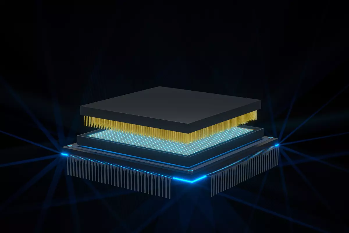
Advanced packaging is a critical component amid growing demand for AI and other data-intensive applications that require compact, high-performance and energy-efficient technology solutions on a single chip. Our next-generation advanced packaging solutions complement our full range of differentiated technologies across our portfolio to provide our customers with an end-to-end solution from design to packaging. With our global manufacturing footprint, we provide the scale and maturity of a world-class manufacturing partner, including the essential enablement and application design kits that accelerate time to market for our customers.

Advanced Packaging and Photonics Center in the U.S.
Our Advanced Packaging and Photonics Center (APPC) in Malta, New York is designed to meet the growing demand for our silicon photonics technology through full turnkey advanced packaging, bump, assembly and testing. We support our customers through providing advanced packaging, wafer-to-wafer bonding, assembly and testing of 3D-integrated and heterogeneously-integrated chips, all under the Trusted Foundry accreditation.

Advanced packaging R&D center of excellence in Singapore
In Singapore, our advanced packaging R&D center of excellence – opened in partnership with Agency for Science, Technology and Research (A*STAR), Singapore’s leading public sector research and development agency – is focused on next-generation photonics and developing capability in chip-stacking and wafer bonding technologies.
Our solutions in Singapore are manufactured on our 200mm silicon photonics platform, with plans to scale to 300mm. The expanded technology portfolio, production capacity and R&D from the Singapore site complements our U.S. capabilities.