Technologies
Feature-rich CMOS
Feature-rich solutions tailored to your application needs, backed by a global manufacturing footprint
Built on advanced planar CMOS platforms, our portfolio balances performance, power and cost while enabling highly-integrated designs through rich embedded functionality. Supported by global manufacturing and options for regional expertise, we provide proven solutions that scale across a broad range of applications.

-
Comprehensive solutions
40+ distinct platforms spanning 10+ nodes from 22nm up to ≥180nm
-
Feature-rich by design
Technologies supporting high-voltage, ultra-low leakage, ultra-low power, embedded non-volatile memory (eNVM) and analog compute-in-memory
-
Designed for system integration
Advanced mixed-signal integration, feature-dense SoCs that reduce system complexity and optimize performance, area and cost
-
Global to local manufacturing
High-volume manufacturing across the U.S., Germany, Singapore and through partners in China, trusted by more than 200 customers worldwide
-
Design once, scale globally
One PDK, one GDS, multi-site qualification for manufacturing across facilities spanning the globe
-
Technology porting
Validated PDKs and IP, robust design enablement and experience in technology porting in close partnership with customers


Proven technologies, faster time-to-market
Design your next breakthrough product with our feature-rich CMOS technologies, engineered for reliable, long-lifecycle designs with global manufacturing and robust design enablement.
-
Serving 200+ customers worldwide
Trusted technology leadership for applications spanning automotive, industrial IoT and other high-growth markets
-
Leading supplier to the #1 automotive MCU player in 2025
More than 2 million wafers shipped on 40nm technology, backed by Auto Grade 0 qualification and reliability
-
eNVM solutions
Including embedded Flash (eFlash) and analog compute-in-memory
-
Custom silicon offerings
Design your custom SoCs with processor IP from MIPS, a GlobalFoundries company
-
Broad IP enablement
Extensive GF-owned and partner IPs, including analog mixed-signal, embedded memory and interface IPs
-
Multi-source manufacturing
40nm production at multiple GF sites, ensuring supply continuity and regional flexibility

Your gateway to smarter, faster & more immersive experiences
Choose the feature-rich CMOS process technology that best fits your sensing, compute or display application requirements.
Our sense technologies, including optical sensor options, enable low-noise, high-sensitivity imaging and sensing designs to power sensor and mixed-signal SoCs and ASICs. Our sense technologies are engineered for reliable signal acquisition across a wide range of sensor front ends – available from 22nm to 130nm nodes.
- Our technologies enable consumer and automotive cameras with high-dynamic-range CMOS image sensors (CIS) and wafer-to-wafer bonding capability.
- CMOS microphone and audio front‑end ASICs deliver best‑in‑class signal‑to‑noise ratios (>75 dB) for high‑performance voice, audio and sensor‑fusion systems.
- Front-side illuminated single photon avalanche diode (SPAD) optical sensor on GF’s 55nm platform enables direct time‑of‑flight (dToF) sensor SoCs for advanced depth‑sensing.
- Our technologies support diverse sensing applications spanning consumer, medical, industrial and automotive markets, including emerging edge AI use cases.
Our compute technologies support cost‑optimized edge processing for scalable MCU with ultra-low power, ultra-low leakage and eNVM capabilities, spanning 22nm to 180nm nodes to address diverse performance, power and lifecycle requirements.
- We enable applications across IoT, industrial, automotive, edge AI and secure connectivity, including automotive MCUs, secure MCUs, edge-connected devices and Bluetooth low energy microcontrollers – including with our newest 22UX and 40UX platforms.
- Unique analog compute- in-memory capabilities on our 28SLPe-ESF3 technology support faster, more energy-efficient processing for AI workloads.
Our feature‑rich CMOS display solutions support a broad range of display driver and micro display backplane applications, enabling reliable operation, low leakage and consistent visual performance across markets – supported across 28nm, 40nm and 55nm nodes.
- We are the first pure-play foundry to produce mobile OLED display driver ICs (DDICs)
- Our 28nm high-voltage (HV) technology features the industry’s smallest SRAM bitcell.
- Our portfolio of display solutions address applications from wearables to automotive environments.
Serving diverse markets with feature-rich CMOS technologies


Scale your designs with our trusted partner ecosystem
Access our global partner ecosystem, with validated IP, EDA and design services expertise across our feature-rich CMOS technologies to accelerate development from concept to production.


Frequently asked questions
Yes, we offer MPW prototyping across all of our technology platforms, including feature-rich CMOS.
Our feature-rich CMOS technologies are manufactured across our facilities in the U.S., Germany and Singapore for supply assurance and regional flexibility.
- 28nm – 300mm: Malta, New York; Dresden, Germany; Singapore
- 40/45nm – 300mm: Malta, New York; Dresden, Germany; Singapore
- 55-90nm – 300mm: Malta, New York; Singapore
- 110-180nm – 300mm and 200mm in Singapore | 200mm in Burlington, Vermont
*Additional manufacturing options available through our manufacturing partners in China. Contact us for further details.
Our feature-rich CMOS portfolio offers support for multiple eNVM options, including embedded Flash (eFlash) and analog compute-in-memory, across select foundational process technologies used across Sense and Compute applications.
Yes. Our feature-rich CMOS portfolio includes Auto Grade 0 and Auto Grade 1-certified options, embedded memories, high-voltage and mixed-signal integration to support reliable, long-lifecycle automotive applications such as MCUs, sensing and in-vehicle compute.
Latest news & insights
-
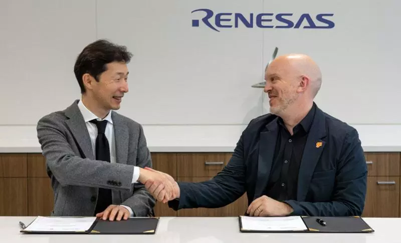
 Learn more: GlobalFoundries and Renesas Expand Partnership to Accelerate U.S. Semiconductor Manufacturing
GlobalFoundries and Renesas Expand Partnership to Accelerate U.S. Semiconductor Manufacturing
-
Learn more: GlobalFoundries and Silicon Labs Expand Partnership to Accelerate Wireless Connectivity Solutions and Strengthen U.S. Chip Manufacturing
GlobalFoundries and Silicon Labs Expand Partnership to Accelerate Wireless Connectivity Solutions and Strengthen U.S. Chip Manufacturing
-
Learn more: GlobalFoundries and Egis Partner to Develop Next-Generation Smart Sensing Technology for Mobile and IoT Applications
GlobalFoundries and Egis Partner to Develop Next-Generation Smart Sensing Technology for Mobile and IoT Applications
-
Learn more: GlobalFoundries and Silicon Labs Partner to Scale Industry-Leading Wi-Fi Connectivity
GlobalFoundries and Silicon Labs Partner to Scale Industry-Leading Wi-Fi Connectivity