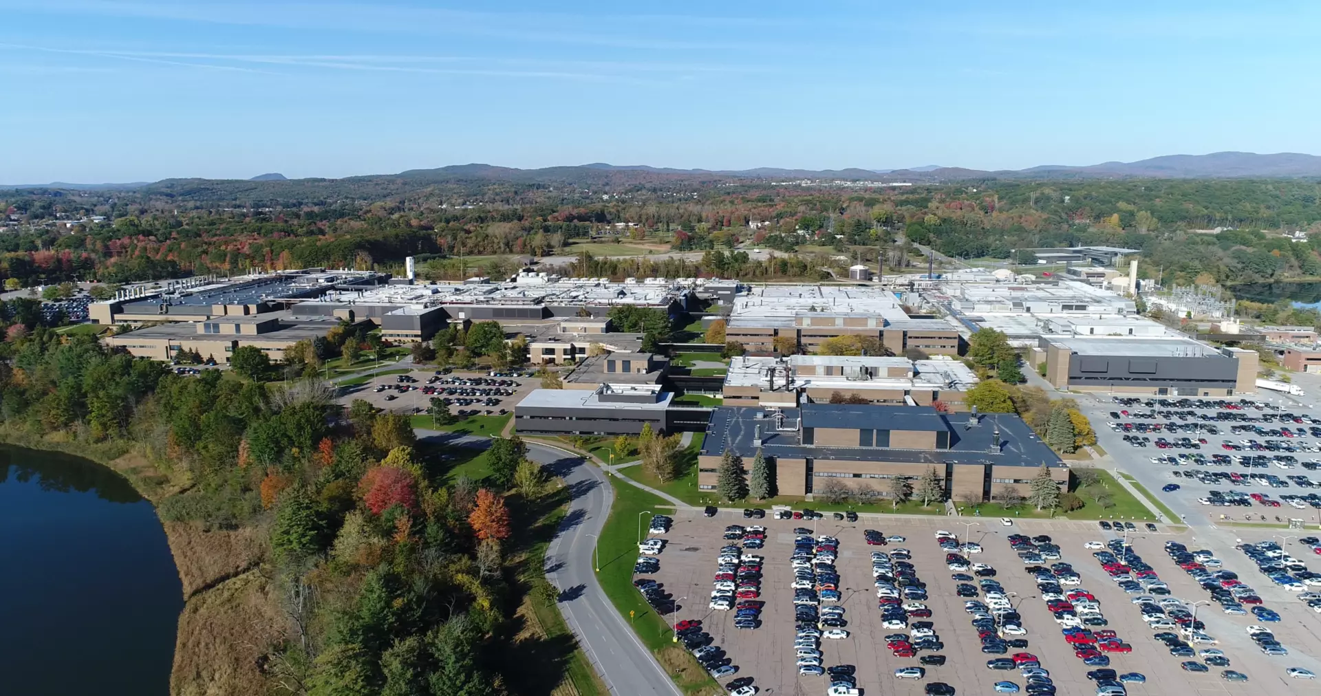
Burlington, Vermont
The GF Burlington site is a global center of excellence for RF and GaN technologies, with decades of expertise supporting high‑performance connectivity and power applications.
Since its founding in 1957, our Burlington site has been a pioneer in specialty semiconductor manufacturing. One of the world’s original 200mm fabs, the site has evolved into a center of excellence for RF-SOI, silicon germanium and gallium nitride technologies.
Acquired in 2015 as part of the IBM Microelectronics business, Burlington supports wireless communications, automotive, defense and critical infrastructure applications worldwide. The site is one of the largest private employers in Vermont and is designated as a U.S. Department of Homeland Security facility.
-
1,800
employees and contractors
-
1957
operations established
-
600k
total wafer capacity per year (200mm equivalent)
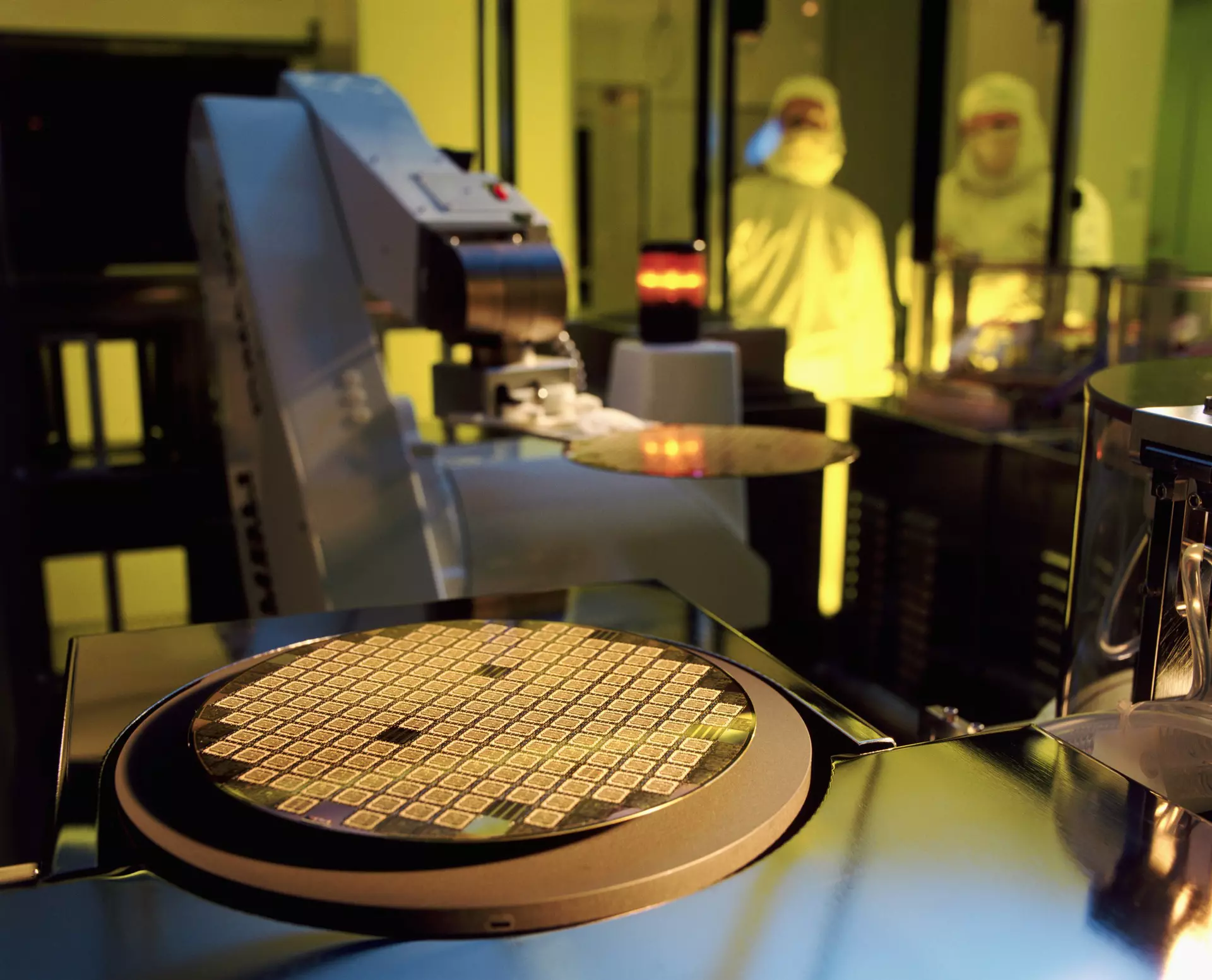
Technologies manufactured here
-

Power BCD
-
RF-SOI
-
SiGe
-
Feature-rich CMOS


Trusted & secure

We play a pivotal role in global security by manufacturing secure semiconductors that enhance the reliability and effectiveness of microelectronics and mitigate the risks associated with counterfeit or untrusted microchips. With a proven track record, we maintain stringent processes, equipment and oversight to ensure the secure production of sensitive chips. We are an Accredited Supplier of the U.S. Trusted Foundry Program – the strongest assurance to produce uncompromised chips for aerospace and defense systems.

AutoPro™ program
With 15+ years of experience serving the automotive market and hundreds of thousands of wafers shipped to date, we have built deep partnerships with leading OEMs and Tier 1 customers. Backed by comprehensive technologies and industry‑accredited fabs around the world, the AutoPro program has a proven track record of meeting and exceeding automotive standards in everything we do.

