Technologies
Advanced packaging
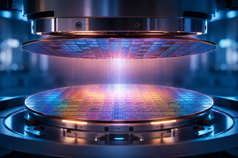
Our advanced packaging services for compact, high-performance and energy-efficient systems integrate multiple technologies to enable new AI-driven architectures.
Scaling next-generation systems
As demand for compact, high-performance and energy-efficient solutions accelerates, advanced packaging becomes critical to enable next-generation systems as traditional scaling approaches reticle limits. Our advanced packaging solutions unify multiple process technologies into a single system, reducing interconnect distances and enabling new architectures across a range of applications.

-
2.5D & 3D integration
Advanced interposer technology enables high-density 3D integration (3DI), flexible wafer-to-wafer (W2W) and die-to-wafer (D2W) bonding for heterogenous integration of logic, memory and power, with through-silicon vias (TSVs) available
-
Integrate leading technologies
Supports W2W and D2W for industry and GF technologies, including our lauded CMOS, RF and silicon photonics platforms, for an integrated solution tailored to your application needs
-
End-to-end integration
Delivers a continuous flow from wafer fabrication to assembly, packaging and test, with optimization, test coverage and full management to our production standards


Integration tailored to your needs
We combine advanced integration technologies, manufacturing expertise and design alignment to enable system-level packaging and production – supporting implementation from development through volume production.
-
3D heterogenous integration
Enables tight integration of multiple technologies and chiplets within a single package to support system-level functionality and performance scaling
-
Homogenous integration
Our SLATE™ wafer-to-wafer bonding technology enables dense integration of similar die for improved interconnect efficiency and form factor scaling
-
Manufacturing expertise
Delivered through our advanced packaging centers in the U.S. and Singapore, enabling secure, end-to-end packaging, assembly and test, all under one roof
-
Design & integration support
Aligns packaging implementation with our technologies and manufacturing flows, supporting system-level integration from development through production
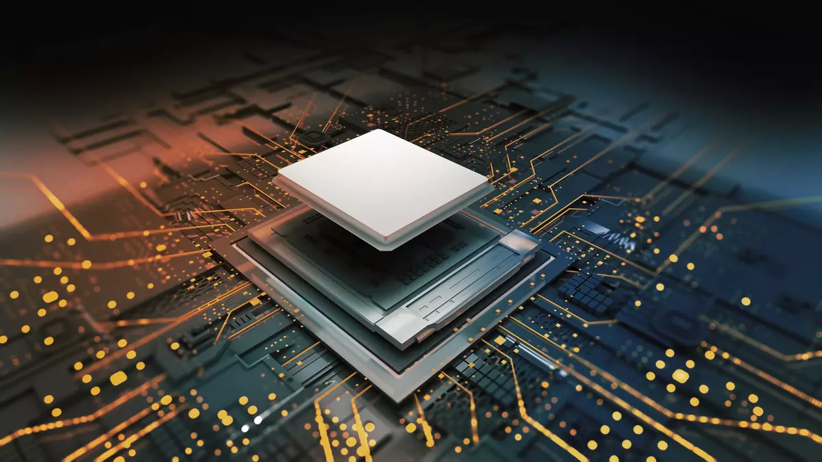
Advanced packaging services
Our advanced packaging services are structured to deliver a complete, end-to-end flow, supported by our dedicated advanced packaging centers, a globally distributed manufacturing footprint and trusted partners complementing our manufacturing for assembly, packaging and test, delivering a streamlined path to production.
-

Interposer/bridges
High-density interconnects between multiple dies using silicon interposers or bridges, with support for stitched and non-stitched implementations, integrates deep trench capacitors for enhanced on-interposer capacitance, enabling high-bandwidth, low-latency system integration
-
Wafer-to-wafer bonding
Advanced bonding technologies, including W2W with dual-wafer bonding fabric for reliable interconnect and SLATE wafer-to-wafer bonding technology for homogenous integration of select GF platforms, deliver dense 3DI and shorter interconnect distances for system-level scaling
-
Die-to-wafer bonding
Supports advanced 3D integration by bonding individual die onto wafers, enabling higher integration density and flexible chiplet-based architectures
-
Thru-silicon vias (TSV)
Enables high-density vertical interconnects for W2W and D2W integration, allowing heterogenous logic, memory and power devices to be interconnected in advanced 3D architectures; within advanced silicon interposers, TSVs provide the vertical electrical path from the top-mounted die through the interposer to the package substrate


Advanced packaging centers
Our advanced packaging centers in the U.S. and Singapore deliver next-generation differentiated silicon-proven solutions for advanced packaging. Our Advanced Packaging and Photonics Center (APPC) in Malta, New York focuses on silicon photonics co-packaged optics (CPO) development and our advanced packaging R&D center of excellence in Singapore specializes in next-generation photonics and developing capability in chip-stacking and wafer bonding technologies.
Advanced packaging applications


Frequently asked questions
Advanced packaging enables tight integration of photonic and electronic components to meet bandwidth, power and form factor requirements. By supporting high-density interconnects, flexible fiber attach, thermal management and 2.5D/3D integration, our advanced packaging services provide the foundation for assembling, testing and deploying complete photonics systems as architectures evolve, enabling scaling from pluggable modules to co-packaged optics (CPO) and more integrated architectures.
Yes. Our U.S.-based APPC center supports secure, onshore manufacturing, packaging and test, enabling trusted supply chain options for sensitive applications.
We support a range of advanced packaging technologies, including 2.5D interposer-based integration with TSV formation and reveal, redistribution layers (RDL) and passivation for signal routing and protection, with W2W and D2W bonding – extending to 3D integration using TSV-enabled stacking.
Advanced packaging’s ability to support heterogeneous integration across multiple technology nodes, including logic, memory and power, are essential to enable evolving AI workloads and high-performance, compact solutions across communications infrastructure, data centers, aerospace and defense, automotive and IoT systems.
Yes. We support the full lifecycle from development and qualification through volume manufacturing, enabling customers to scale designs from concept to production.
Latest news & insights
-
Learn more: Unlocking smaller, smarter RF front-ends with SLATE™ advanced packaging technology on 9SW
Unlocking smaller, smarter RF front-ends with SLATE™ advanced packaging technology on 9SW
-
Learn more: GlobalFoundries qualifies SLATE™ advanced packaging technology on 9SW platform for next-generation radio frequency applications
GlobalFoundries qualifies SLATE™ advanced packaging technology on 9SW platform for next-generation radio frequency applications
-
Learn more: How GlobalFoundries is manufacturing quantum at scale
How GlobalFoundries is manufacturing quantum at scale
-
Learn more: GlobalFoundries partners with A*STAR to accelerate advanced packaging innovation
GlobalFoundries partners with A*STAR to accelerate advanced packaging innovation