By: Alex Margomenos, senior director, RF-SOI product line
Modern smartphones must maintain strong radio performance across dozens of frequency bands, ranging from a few hundred MHz up to 7 GHz, to support 5G new radio (NR). At the same time, antenna performance is highly dynamic – affected by factors such as distance to base station, device orientation, proximity to the human body or metallic surfaces and hand placement. Conventional smartphone antennas, such as Printed Inverted-F Antennas (PIFAs), typically have a narrow bandwidth of about 10%, which would otherwise require many antennas to cover the entire frequency range across all operating conditions.
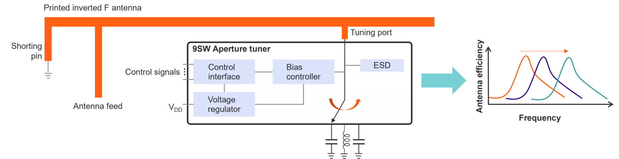
That is where antenna aperture tuners come to the rescue. These circuits dynamically adjust the electrical length of the antenna, enabling efficient operation across multiple bands. Antenna aperture tuners are typically part of a closed loop control system that uses inputs from the modem, sensors and RF power detectors to select and optimize antenna performance in real time.
The primary objective of antenna tuning is to maximize the total antenna efficiency, which is a metric of how much of the power generated in the smartphone transceiver is radiated from the antenna. Tuners achieve this by switching capacitors and inductors to modify the antenna’s electrical length. This is implemented through specialized RF switches placed at key points along the antenna.
When RF signals are fed to the antenna, they create a voltage and current standing wave pattern with peaks and nulls. The location of these depends on the frequency of the signal, the length of the antenna and the type of terminations on each edge of the antenna (for a typical PIFA, one edge is shorted to the ground and the other is open). For maximum effectiveness, tuners are ideally placed at voltage peaks, although practical design constraints may limit optimal placement.
Placing antenna tuners at the voltage peaks means that these switches need to handle high peak voltages – often exceeding 80V near the open end of the antenna. Key switch parameters, such as on-resistance (Ron) and off-capacitance (Coff), influence efficiency differently depending on location: Ron dominates in high-current regions, while Coff becomes more critical in high impedance regions, closer to the open termination.
RF-SOI technologies have been the key enabler of aperture antenna tuners because they can address all key requirements. Built on trap-rich, high resistivity substrates, RF-SOI offers low harmonics, low substrate parasitics and ability to stack multiple field effect transistors (FETs) to achieve the required high Vmax. Ongoing process improvements and scaling has reduced the Ron×Coff product and enabled smaller switch die sizes.
GlobalFoundries’ (GF) 9SW, our fourth generation RF-SOI platform, is designed to meet these requirements. Our industry-leading 9SW technology is based on 90nm back-end-of-line (BEOL) lithography, offering multiple switch options with both standard and thick gate oxide optimized for low Ron*Coff and high voltage handling. The platform includes a full suite of logic and high voltage analog FETs as well as a large variety of capacitor and resistor options ideal for capacitive compensation, bias control and body current management of large switch stacks. This September, we are introducing improved switch versions coupled with enhanced metal routing capabilities, offering improvements in Ron*Coff with tighter switch pitch while maintaining excellent voltage handling capabilities for our 9SW platform. These new unique capabilities enable next-generation antenna tuners while simultaneously achieving low Ron*Coff and voltage handling at a smaller switch die size.
Additional die size reduction is achieved by our production-ready SLATE™ wafer-to-wafer bonding technology with 9SW, which bonds two 9SW wafers to enable three-dimensional circuit folding. This approach reduces die area by up to 45% without compromising performance. Our latest PDK incorporates design enablement tools that allow designers to intuitively migrate two-dimensional circuits to three dimensions, accelerate prototyping and reduce design cycles. Watch our tutorial video and read the blog to learn more about our SLATE wafer-to-wafer bonding technology with 9SW and PDK capabilities.
To further support design optimization, GF provides reference designs and guidelines that help better balance voltage distribution across large switch stacks, optimize layout and enhance ESD robustness.
Contact your GF representative to learn more about our solutions for antenna tuners with 9SW and 9SW SLATE, as well as the rest of our RF portfolio in RF-SOI, SiGe and RF GaN.