Over 150 years ago, James Clerk Maxwell proposed an idea that even some of the era’s leading scientists struggled to accept. A changing electric field, he argued, could produce effects similar to electrical current, even when no charged particles were physically moving. Known as displacement current, the concept would become one of the foundations of modern electromagnetism, helping explain how electromagnetic waves, including radio waves and visible light, propagate through space.
Semiconductor innovation has largely been driven by a different mechanism: moving electrons. From the transistor to the smartphone processor to the AI accelerator, progress has come from controlling the flow of charge through ever-smaller devices. But RF engineers have run into a different problem. As RF switches shrink, unwanted effects such as parasitic capacitance and contact resistance begin to dominate, and at advanced process nodes those parasitics can overwhelm the benefits of scaling.
That realization led Dr. Mohammad Samizadeh Nikoo and Hua Wang, professor of electrical engineering at ETH Zurich, to ask a question: what if the next breakthrough in RF switching did not come from optimizing another transistor? Instead of relying on conventional transistor operation, they designed a switch that uses displacement fields and quantum tunneling currents, drawing on a mechanism rooted in Maxwell’s original framework.
The research was conducted while Nikoo was a postdoctoral researcher in Wang’s IDEAS Group at ETH Zurich. Nikoo is now an assistant professor at Nanyang Technological University in Singapore. Their findings were published in January 2026 in Nature Electronics in a paper titled “High-power millimetre-wave switches on silicon using displacement fields and tunnelling currents.”
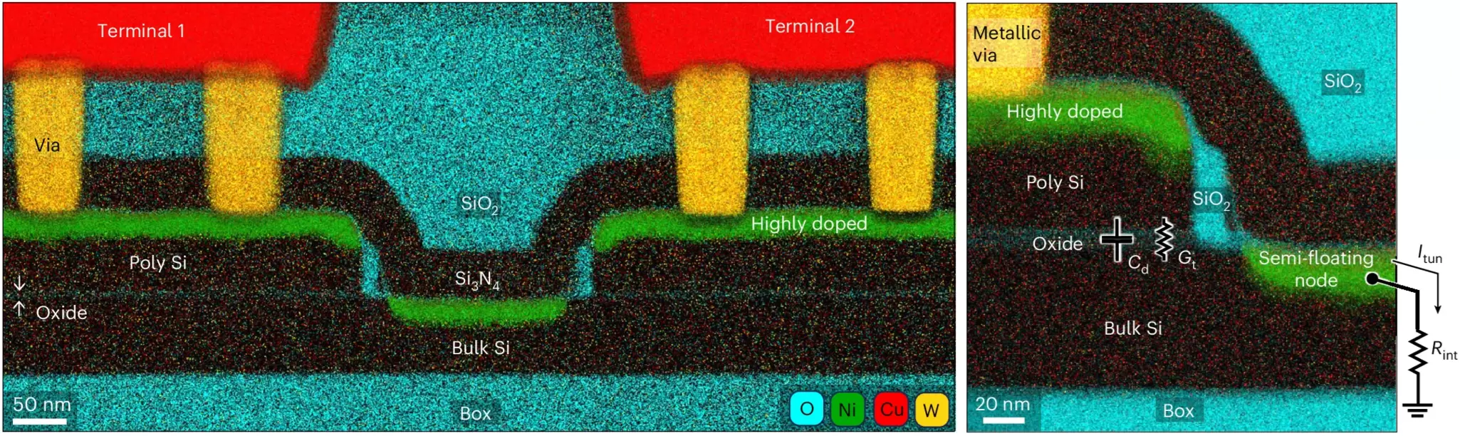
Turning the idea into a working device took more than a promising theory. Wang’s group has built an extensive partnership with GlobalFoundries through GF’s University Partnership Program, which gives university researchers access to advanced GF technologies along with design and technical support. The team built the switch on GF’s commercial 45nm RF-SOI platform using a “zero-change” approach — no custom fabrication, no specialized manufacturing flow, just elements of an existing commercial process assembled to operate through a different physical mechanism. Wang notes that the clean substrates and low parasitics of GF’s CMOS SOI technology were key to the device’s success.
The results were striking: sub-30-picosecond switching, more than 10 times higher power handling than conventional transistor-based switches on the same platform and significant gains in linearity and parasitics.
We spoke with Nikoo and Wang about why RF hit a wall, what changes when you switch with fields instead of electrons and where a device like this could end up. The conversation has been edited for length and clarity.
Why can’t RF just keep shrinking the way logic does?
Dr. Mohammad Samizadeh Nikoo: The performance metrics of a transistor don’t improve anymore if we just make them super small. For transistors, we normally get the best performance when the gate length is 25 or 30 nanometers, because beyond that we become completely limited by the parasitics. The contact performance between metal and semiconductor limits the conductance of the device, and at the same time the contacts are closer together, so the parasitic capacitances become larger and larger. We don’t gain, we lose. That’s why at some point there is no improvement in performance. It really has very fundamental limitations. Here I call it a change of paradigm, because we are not talking about optimization of a transistor. This is a fundamentally new device working on completely different mechanisms. We don’t transmit the signal by injecting electrons; we use fields to transmit the signal which is why we can get better efficiency, higher power and faster speed.
When you say better performance, how much better — and what does that give an end user?
Nikoo: There are four things. First, parasitics: the switch outperforms conventional switches on the Ron·Coff figure of merit, which is independent of scaling, so it shows how good the technology itself is. Fewer parasitics means you can switch higher frequencies. Second, linearity, measured by IIP3. If you’re switching a communication signal for modulation or beamforming, you need the switch to be very linear in the on state so frequency components don’t mix and degrade signal quality. Here we’re talking about 17 dB. That’s two orders of magnitude higher linearity and power. Third, power capability: more than an order of magnitude higher. You can never get 25 dBm from a single transistor. People need power combining and a lot of other things that take a big footprint, and here a single device does it. And fourth, switching time. Sub-nanosecond switching is already quite impressive for a switch, and here we are talking about sub-30 picoseconds. Those four things together make it a very promising solution.
Why was it important to demonstrate this on a commercial RF-SOI platform?
Professor Hua Wang: People have been looking at new devices and giving heroic, record-breaking performance, but many of them are ad hoc and use dedicated processes. The device is great, but it has limited scalability, yield and manufacturability. That’s exactly why we wanted to use what we call a zero-change approach: use the existing commercially available technology platform but demonstrate new devices. By doing so, what has been demonstrated here will have large scalability and manufacturability. Using these existing commercial technologies also allows the new devices to be co-designed, co-integrated and co-operated with conventional devices and more standardized RF circuits and systems, which further expands their capabilities. If we want to set a new scientific record, a single device is good. But if we want to address real practical challenges, we have to design functional circuits and systems for a real application.
Where could a switch like this actually be used?
Wang: Two major categories. One is a wide variety of reconfigurable circuits at terahertz and beyond, for joint communication and sensing. We want to go to higher frequency for more bandwidth, higher spatial resolution and low latency, but it’s very hard to make things reconfigurable because we don’t have high quality switches at that frequency. That’s true not just for RF electronics but for reconfigurable antennas and reconfigurable intelligent surfaces. With this technology, all of those systems become possible. The other is wireline and serial data — the data center and AI. A big part of that is how we modulate electronic data at very high speed onto a photonic waveguide, and that invariably requires high-performance switches with low loss and very fast on and off time. AI is a connectivity problem. It’s connectivity in terms of bandwidth and connectivity in terms of energy efficiency.
What does this mean for silicon as 6G moves to higher frequencies?
Nikoo: For 6G and future wireless systems, people investigate new materials. We know silicon is great. It provides integration capability that we never had with gallium nitride. But people look into gallium nitride and its integration with silicon, and they are willing to make the process more difficult to get the advantage of higher power capability. Here, we use a new technology on silicon that can do things we could usually only do with gallium nitride, which is the superior material. I think this really changes the chance for silicon to still remain as the dominant platform for future wireless.
What’s the benefit of working with GF’s University Partnership Program on research like this?
Wang: We benefit tremendously from this relationship with GlobalFoundries. Not only are we offered really advanced technologies and a lot of design and technical support and advice, but I also want to comment on the technology itself from GF. We are using the GF CMOS SOI technologies, and the clean substrate of SOI and the lowest parasitics is also a key factor for the success of this device.
Nikoo: Having access to this process through a partnership between GF and the university also gives university groups the chance to try more risky ideas, which is sometimes difficult if you have very limited space — something that is more high risk, high gain. With a new project style, we need to deliver KPIs and a lot of things, and that reduces the flexibility we have to try sometimes very interesting ideas. So I think this is also something quite helpful. The device community and the circuit community are two distinct communities, and sometimes they don’t quite understand each other. There have been important device developments that never became useful, practical things in industry because they rely on manual processes. What we did here is at the interface of those two communities. We made a new device, but on a platform that can be directly used by circuit people, and that increases the impact.
What’s the next phase of this work?
Wang: Nikoo is now leading his group at NTU in Singapore, and his focus is more on devices — he already has a variety of projects further pushing the device innovation side of this concept. On my side at ETH, we are more of a circuit and system group, so we are looking at adopting this device into more complex systems and circuits, for example the reconfigurable terahertz circuits we just talked about. Basically, we want to put it into real use.