Manufacturing
Manufacturing services
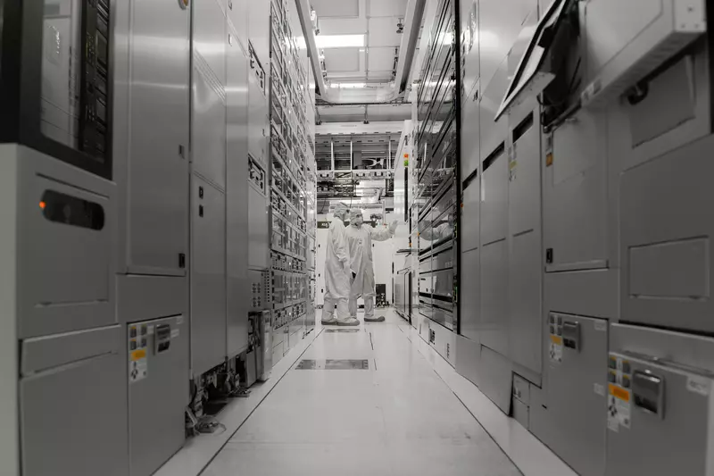
Leap from the starting line into a powerful finish when you partner with GF
Every product starts from an idea, and you deserve a manufacturing partner that knows how to support you the entire way. Our manufacturing services are designed to seamlessly get you from chip design to wafer fabrication to final assembly and test. With the advantages of a global footprint and a leading reputation in semiconductor manufacturing and testing, we make it easier for you to follow through on process so you can create the most effective product for your customers. Wherever your idea is headed, let us help you get it to the finish line.
-
Global
manufacturing footprint
-
RF testing
leadership
-
25+
years of experience

Global network of partners
Located worldwide, our OSAT partners have been vetted and approved by GF so our customers can be confident in their products, from beginning to end.

World-class test solutions provider
A leader in complex testing, we have developed over 600 test solutions that provide customers with the reliability assurance they need at every stage of production.
- Extensive RF testing solutions
- High and low temperature test capabilities
- Analog and digital TxRx testing
- Memory testing including eNVM
- High-speed interface test capabilities
- High-voltage and high-current testing
- ATE test programs

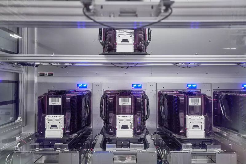
Wafer services
As part of a full turnkey offering, we offer bump, wafer level package and probe capabilities, complemented by OSAT partnerships, to provide a one-stop-shop for customers’ wafer needs. Creating a reliable and high-quality path to production, we streamline manufacturing so customers can realize their designs quicker.
- Bump offerings for 200mm and 300mm, including SnAg bump, copper pillar and WLCSP
- Wafer sort with Known Good Die methodology
- Backside grind, wafer sort and bake, dicing, marking and binning services available
Module services
Comprehensive, reliable and supported by OSAT partners, our module services convert manufactured wafers into customized products with flexible packaging options.
- Industry-standard packaging including scan bake tape
- Package and assembly capability complemented by trusted OSAT partners
- Test offerings: Complex RF tests, burn-in testing for early signs of failure and module final testing for pre-board certainty

Engineering services
From design to product packaging and testing needs, our engineering services go beyond standard manufacturing practices to deliver the solutions that enable unique ideas to become reality. For questions of design feasibility, connectivity enablement and package resilience, we have the experience and partnerships to address the specific questions customers need answered.
- Work with our partners to perfect your design for manufacturing with our design services
- Package engineering services, including electrical analysis, thermal analysis and mechanical analysis
- Wide range of reliability stress services to meet client qualification needs consistent with JEDEC, Mil-std and AEC specifications
- Engineering and debugging services available for all GF tests in production, including customer-written test programs
- Choose from a range of test solutions including extensive state-of-the-art RF, analog and digital testing solutions backed by 22 years of high-frequency mmWave test experience
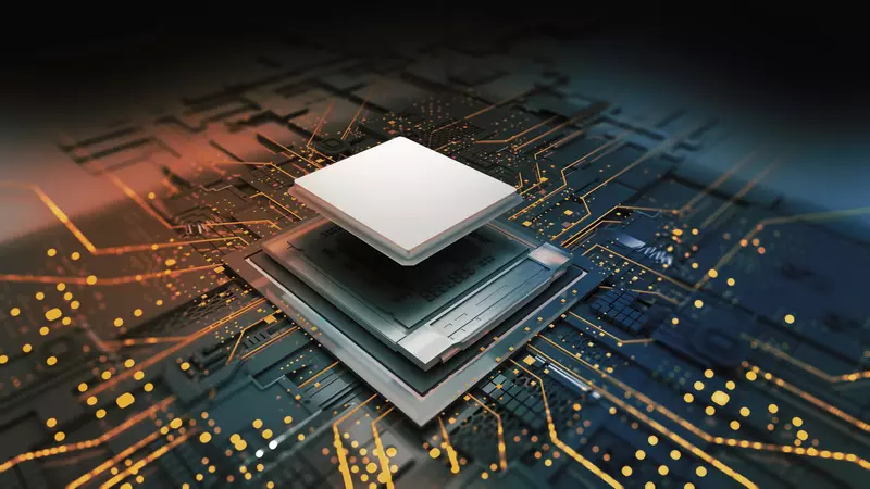
Advanced packaging services
To meet the growing demand for silicon photonics and 3D and heterogeneously-integrated (HI) chips, our advanced packaging solutions in both Malta, New York and Singapore are designed to provide a full suite of differentiated solutions for our global customer base. Find out more about our advanced packaging solutions here.