Payne’s perspective on showcasing beauty, complexity and the future in semiconductor manufacturing
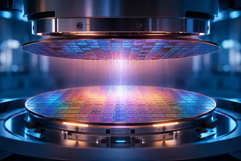
In late 2022 GlobalFoundries (GF) invited Chris Payne, an acclaimed photographer with a specialization in architectural and industrial photography, to our Malta, New York, facility for a behind-the-scenes glimpse into the world of semiconductor manufacturing. Over the course of six days, he captured dozens of images, showcasing the intricate processes of GF’s cleanroom, sub-fab and other key areas. Several of these striking images are featured in Payne’s recent book, ‘Made in America’ and are now proudly displayed in the ‘Semiconductors Unveiled’ gallery at our headquarters. We recently caught up with Chris to ask him about his creative journey at GF and how his photography bridges art with the cutting-edge world of semiconductor technology.
Q: Thanks so much for connecting, Chris. Your latest book ‘Made in America’ includes a section on semiconductor manufacturing. What inspired this focus?
A: In my book I wanted to tell a comprehensive story about manufacturing, drawing a narrative arc from older, more traditional processes to newer, more technologically advanced ones, like the making of semiconductor chips. Being able to photograph GlobalFoundries was like having the final chapter written and made it easier to assemble the rest of the book.
Q: How did your perception of the company evolve throughout your photographic journey?
A: Walking into the giant cleanroom for the first time was overwhelming and I realized that I would need help from GF to plan and make the pictures. I couldn’t have asked for a better partner; the shoots felt like a creative collaboration where we all shared a common goal. This level of cooperation and generosity is rare in an age when tech companies are wary of opening their doors to photographers.
Q: Before visiting GF, what were your main objectives or hopes for the photography project? How did these goals shape your approach?
A: My main objective was to make a series of compelling pictures that strike a balance between beauty and information, that pull back the curtain on the chipmaking process while also being aesthetically pleasing. I tried to avoid the generic views we’ve seen before of cleanrooms with workers in white bunny suits. For my pictures I knew I needed to dig deeper, so we spent many hours exploring the fab to come up with new and interesting ideas.
Q: Can you describe the process and any unexpected hurdles you encountered photographing in GF’s semiconductor fab?
A: As a photographer, I’m accustomed to an immersive, hands-on approach, but this wasn’t possible at GF since I was suited from head to toe in protective gear. Every piece of my equipment had to be wiped down before entering the fab, and we had to budget extra time to get around such a vast and labyrinthine site. That said, I enjoyed the luxury of widespread access and had all the help I needed from the GF team, so things couldn’t have gone smoother.
Q: Was there anything about GF or semiconductor manufacturing that surprised or intrigued you during your visit?
A: What I found most intriguing was the contrast in scale between the miniscule size of the chips and the immense size of the factory. I can’t think of another product or process where this relationship is so disproportionate. I’ve seen cleanrooms before, but I had no idea how much infrastructure is required to make it all work.
Q: Of all the images you captured at GF, which one do you find the most aesthetically striking, and which is your personal favorite?
A: If I had to choose one picture, it would be the view looking up at the FOUPs (Front Opening Unified Pods) running along the AMHS (Automated Material Handling System). I remember when I first saw the FOUPs zipping overhead I felt as if I had walked into the future. For this picture we were able to choreograph the FOUPs by slowing them down and rerouting them to create a bustling intersection.
Another personal favorite is the image of [GF senior engineer] Lydia inspecting the wafer sorter. Here I was able to place my camera inside the sorter and have Lydia peer inside to create a dramatic, intimate scene. Even though the fab is mostly automated, humans must keep a watchful eye to ensure that everything runs smoothly.
Q: Semiconductor manufacturing is rarely seen as a subject of fine art. How did you approach revealing the beauty in this technical and industrial process?
A: It’s impossible to photograph semiconductor chips being made, since the process is inaccessible and hidden from view, but I knew there had to be a way to convey its complexity. I recall my disappointment when we toured the sub fab because it seemed generic, like any other mechanical space. Then I looked up and saw a maze of pipes and tubes feeding the cleanroom, revealing the fab as one giant interconnected machine. It was the perfect balance of order and chaos, yet still ambiguous enough to inspire imagination and awe, and shows that beauty can be found in the most unexpected of places.
Q: How do you think your work, particularly in semiconductor manufacturing, influences public perception or understanding of this industry?
A: I’d like to think that I’m doing important work, documenting one of the most essential technologies of our time. If my pictures make people pause to appreciate what it takes to sustain our modern, digital way of life, then that’s a bonus. But even if no one notices or cares, I’m still grateful for having seen this incredible place, and look forward to future collaborations with GlobalFoundries!