Technologies
Silicon photonics
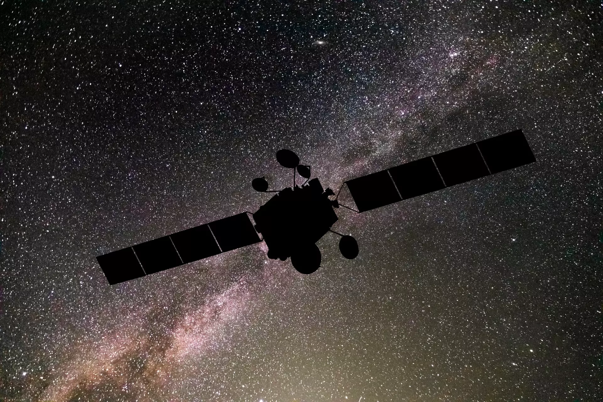
Achieve energy-efficient transmission at the speed of light with our silicon photonics process technologies that enable today’s pluggables and are ready for the ongoing transition of co-packaged optics (CPO).

Fueling the future of electro-optical design with silicon photonics
Built on a scalable, production-proven platform, our silicon photonics process technologies enable high-bandwidth, energy-efficient optical interconnects through tight integration of photonics, RF and advanced packaging to support evolving data center architectures and quantum computing.

-
Supports all form factors
Ranging pluggable optical transceivers, including coherent and long-haul optics, retimed and linear drive pluggable optics (LPO), near packaged optics (NPO) and co-packaged optics (CPO)
-
Extreme design flexibility
Supports custom, semi-custom and standard photonics flows, with the option for integration with our SiGe technology under one roof, enabling highly integrated designs optimized for both slow-and-wide and fast-and-narrow interface architectures
-
OCI MSA-capable interconnect
Our SCALE™ CPO solution for slow-and-wide, scale-out applications meets and exceeds the current Optical Compute Interconnect Multi-Source Agreement (OCI MSA) requirements
-
Flexible fiber attach
GF and ecosystem partner support for permanent, passive attach using undercut (v-grooves) and non-undercut solutions as well as detachable solutions, supporting broadband and high-power optical applications
-
Global manufacturing
We offer 300mm and 200mm manufacturing at scale across our Malta, New York and Singapore facilities, backed by in-house packaging and test resources
-
Advanced packaging
Solutions including TSVs, sub‑100 µm Cu pads, detachable fiber attach and support for advanced‑node EIC and on‑die lasers (in development), with U.S. onshoring planned at our Advanced Photonics & Packaging Center Malta, New York


High-performance, scalable photonics solutions
Our silicon photonics technologies deliver the performance, bandwidth scaling and energy efficiency required for today’s pluggables and next-generation CPO architectures.
-
Proven to 200G/λ, clear path to 400G/λ
Bandwidth upgrades optimized for demanding data center architectures and AI/ML clusters
-
Turnkey design enablement
Through our qualified platforms, PDKs, reference flows and a proven partner ecosystem – accelerating first-time-right design and volume production
-
Demonstrated athermal CWDM filters
With <1dB insertion loss, <0.2dB passband ripple and <-30dB crosstalk. Reliable, low-loss optical links with reduced signal degradation for low-latency, energy-efficient interconnects. Intrinsic EMI immunity helps minimize crosstalk and preserve signal integrity (*design dependent)
-
8/λ and 16/λ bi-directional DWDM
We are the only 300mm silicon photonics foundry that has demonstrated 8λ and 16λ bi-directional DWDM natively on our platform, dWDM filters with 100-400GHz channel spacing are available

Introducing our SCALE™ CPO solution
Our SCALE™ CPO solution is the industry’s first OCI MSA‑capable platform, exceeding requirements for the interconnect specification for modern AI scale‑up architectures. Built on advanced silicon photonics, this future-proofed solution combines integrated photonic devices, CWDM and DWDM and advanced packaging to improve bandwidth density and system scalability – versus traditional copper – for next‑generation optical compute interconnects.
-
Fiber attach & optical scalability
Broadband detachable fibers with flat insertion loss over the CWDM spectrum to future-proof scaling from 4λ in each direction to 8λ and beyond, while enabling serviceability and known-good-die testability for next-generation AI interconnects
-
Photonic portfolio strength
Advanced portfolio of fully-qualified photonic devices, such as 50Gbps and 100Gbps micro-ring modulators, coupled ring resonators and integrated photodiodes
-
Advanced packaging enablement
Support for TSVs for high-speed signaling, power delivery and copper pad pitches ranging from 110µm down to sub-45µm for 2.5/3D stacking from organic substrates to silicon interposers
-
Electronic-photonic integration
Integrates electrical ICs on single-digit advanced nodes to optimize best-in-class compute and state-of-the-art optics without compromising performance

Silicon photonics at-a-glance
Build on our flagship silicon photonics process technology to enable scalable data center architectures, matched to your data capacity and fiber utilization needs.
Our widely adopted, first-generation silicon photonics process technology delivers production-proven, high-volume capability to support up to 100G/λ. By enabling flexible channel spacing (100–400GHz) and 55GHz bandwidth, this process technology is optimized to enable advanced modulation for highspeed interconnects and scalable data center networks.
Proven up to 200G/λ with significant bandwidth upgrades (>65GHz), 200GHz channel spacing and optimizations for advanced modulation formats, our second-generation silicon photonics technology delivers double the bandwidth per wavelength to support growing data center and AI/ML architectures.
Our next-generation silicon photonics process technology offers a clear path 400G/λ, optimized for scale across data center architectures. Early access is now available – contact us to explore co-development opportunities with GF.
Delivering a new era of data transmission with silicon photonics
Billions of connected devices and increased data center power consumption are driving the need for innovative solutions that move data faster and more efficiently than traditional copper cables. This is where silicon photonics technology is critical – enabling higher data rates, super-charging fiber-optic communication networks to fuel high-bandwidth, low-power optical interconnects for leading-edge data center products.


GF business webinar series: GF at the forefront of the photonics & packaging revolution
This webinar showcases how our differentiated platforms and high-performance interconnect technologies are addressing the need for increasing levels of speed, efficiency and scalability for next-generation data and connectivity applications.
Scale your designs with our trusted partner ecosystem
Our expansive ecosystem is your gateway to end-to-end, photonics-specialized partners versed in advanced photonics flows – from fab to fiber – matched to your unique system requirements.


Breakthrough in wafer-level detachable fiber connector solutions with SENKO
Explore how we are advancing scalable silicon photonics by combining our process technology with integrated SEAT™ and MPC solutions from SENKO Advanced Components. This collaboration enables precise mechanical alignment, detachability and repeatable optical coupling from wafer-level testing through packaged photonic engines – supporting earlier identification of known good die, improved manufacturing efficiency and a more practical path to co-packaged optics at scale.


Scaling next-generation optical connectivity in collaboration with Corning
We are pushing the bounds of photonics for next-generation CPO architectures in collaboration with Corning by integrating our silicon photonics technology with Corning’s GlassBridge™ glass-waveguide-based detachable fiber connector solution. This partnership supports detachable, low‑loss, high‑bandwidth optical coupling compatible with our v‑groove‑enabled photonics platform – enabling greater flexibility, serviceability and a scalable path to co‑packaged optics for AI data center applications.
Silicon photonics applications


Frequently asked questions
Pluggable optics offer modularity, established standards and ease of deployment, while CPO can deliver higher bandwidth density and improved power efficiency by reducing electrical interconnect distance. Our silicon photonics technology supports both approaches, enabling customers to deploy pluggables today while enabling the ongoing transition of CPO architectures as system requirements evolve.
- Support for pluggable optics: Our production-proven silicon photonics process technology is ready for immediate deployment, with support for passive fiber attach and barium titanate (BTO) integration for standard pluggables as well as LPO and LRO modules.
- CPO enablement: We offer copper compatible features including Cu pads and μpillars, advanced integration of silicon photonics with SiGe and support for CWDM and multi λ DWDM architectures. These capabilities form the foundation of our SCALE CPO solution, the industry’s first OCI MSA capable platform, and are optimized for both scale-up and scale-out data center models.
We offer silicon photonics packaging, assembly and test through our Advanced Packaging and Photonics Center (APPC) in Malta, New York and Advanced Packaging R&D center of excellence in Singapore.
Our silicon photonics technology is proven to deliver 100–200 G/λ, depending on the generation, with device libraries supporting 56–112 Gbaud classes using 300 GHz-class RF CMOS.
Detachable fiber attach separates optical assembly from wafer processing, improving manufacturability, test and serviceability across production flows. By enabling multiple fiber‑attach approaches, it also gives system designers greater flexibility to adapt packaging, form factors and deployment models as optical architectures scale. Our in-house capabilities and our ecosystem partners support both direct and detachable fiber attach, including v‑groove‑based attachment and scalable packaging flows.
We offer scalable 300mm manufacturing across our Malta, New York and Singapore facilities – with 200mm manufacturing now available in our added Singapore facility.
Standards and multi‑source agreements (MSAs) help align device, system and packaging requirements across the photonics ecosystem, reducing risk and accelerating adoption. We actively support industry standards efforts, including Optical Compute Interconnect Multi‑Source Agreement (OCI MSA) initiatives, to ensure our silicon photonics platforms are interoperable, scalable and ready for next‑generation optical architectures.
In addition to AI and cloud infrastructure, our silicon photonics technology is well suited for applications such as high-performance computing, LiDAR, industrial automation, sensing and emerging optical compute architectures where high bandwidth and energy efficiency are critical
Latest news & insights
-
 Learn more: Keysight Expands Photonics Design Ecosystem with GlobalFoundries PDK (opens in a new tab)Jun 3, 2026
Keysight Expands Photonics Design Ecosystem with GlobalFoundries PDK
- Learn more: GlobalFoundries joins U.S. Department of Energy's Genesis Mission as industry partnerJun 3, 2026
GlobalFoundries joins U.S. Department of Energy’s Genesis Mission as industry partner
- Learn more: Sivers & GlobalFoundries Advance AI Data Center Optical Solutions (opens in a new tab)Jun 2, 2026
Sivers & GlobalFoundries Advance AI Data Center Optical Solutions
- Learn more: From electrons to photons: Scaling optical connectivity with silicon photonics and SiGeMay 12, 2026
From electrons to photons: Scaling optical connectivity with silicon photonics and SiGe