
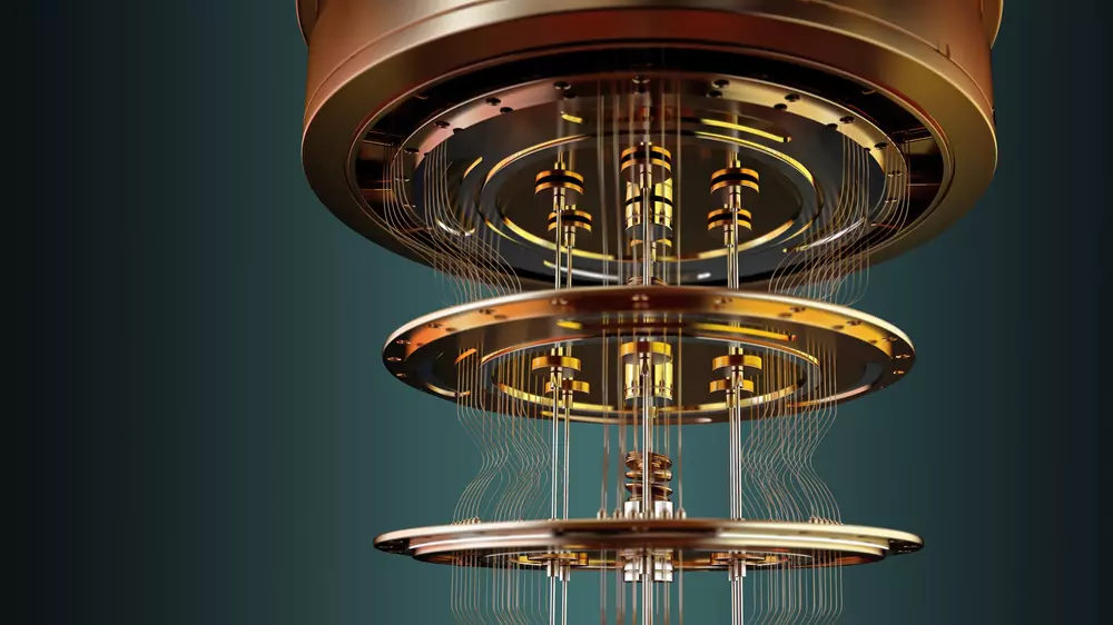
技术
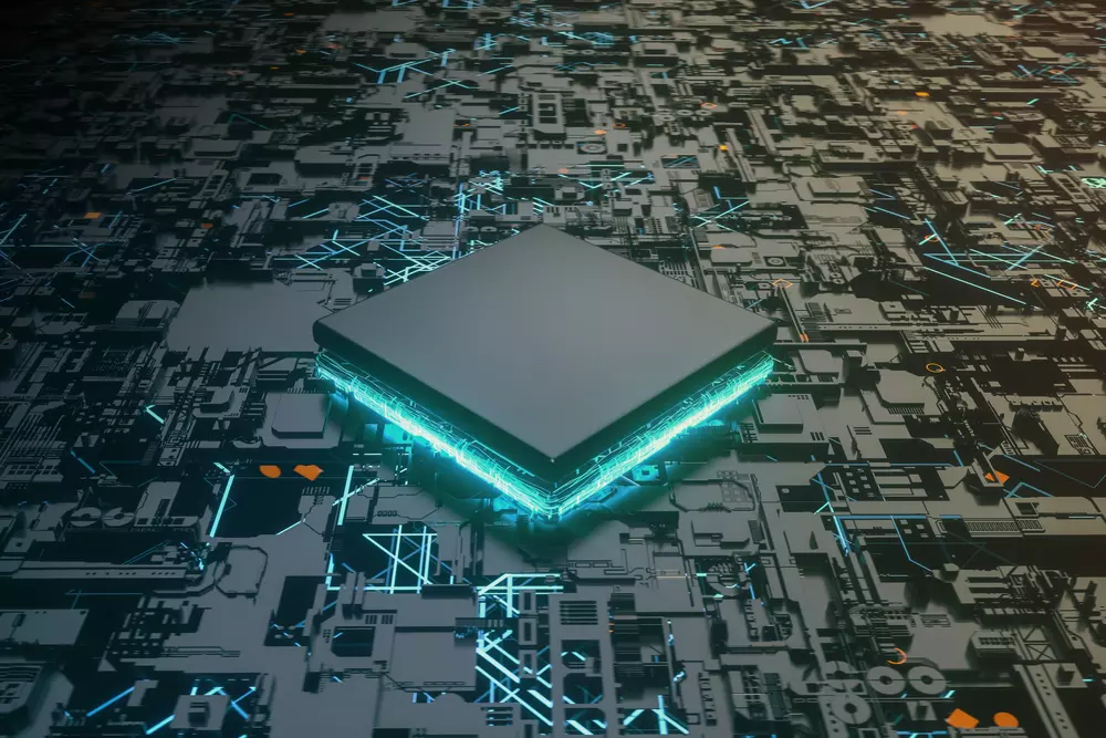


卓越制造,全球与本地并重

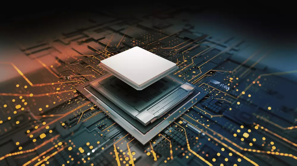
凭借核心技术服务于多元化的市场


最新资讯与见解
-
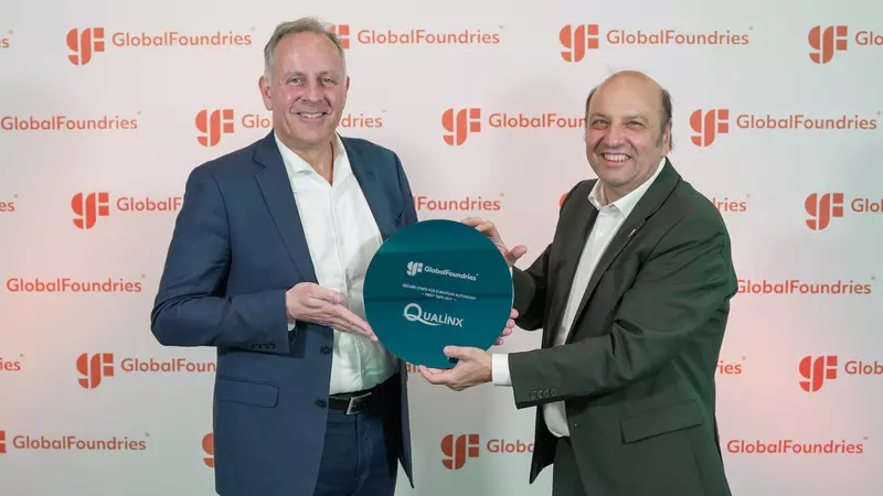
 了解更多:GlobalFoundries 与 Qualinx 展示了欧洲首个针对安全关键型半导体的自主制造流程2026年6月10日
格罗方德与Qualinx展示了欧洲首个针对安全关键型半导体的自主制造流程
- 了解更多:提升射频功率与效率:GF如何将射频GaN技术应用于系统级应用2026年6月8日
提升射频功率与效率:GF如何将射频GaN技术应用于系统级应用
- 了解更多:是德科技借助 GlobalFoundries PDK 扩展光子学设计生态系统 (在新标签页中打开)2026年6月3日
是德科技借助格罗方德的PDK扩展光子学设计生态系统
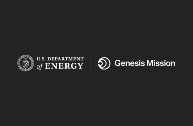
- 了解更多:GlobalFoundries作为行业合作伙伴加入美国能源部的“创世计划”2026年6月3日
格罗方德作为行业合作伙伴加入美国能源部的“创世计划”


GF Connect 门户
与GF合作,比以往任何时候都更快速、更轻松地管理您的订单。访问与设计、工程、质量、生产和物流相关的应用程序及信息。
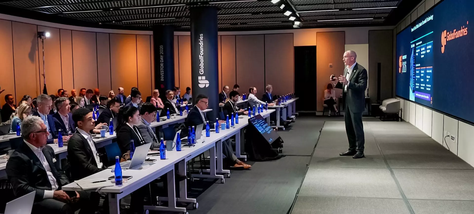
我们塑造重要的东西
关键芯片是现代生活的基石,而我们正是这些芯片的制造者。GF 是一家具备差异化优势的技术合作伙伴,凭借遍布全球的灵活布局,将研发、知识产权、设计、定制芯片与先进制造能力融为一体。依托与客户、政府及生态系统合作伙伴建立的深厚合作关系,我们助力实现最重要的目标。