

技术
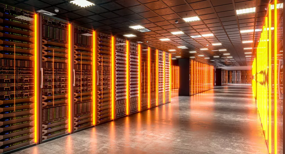


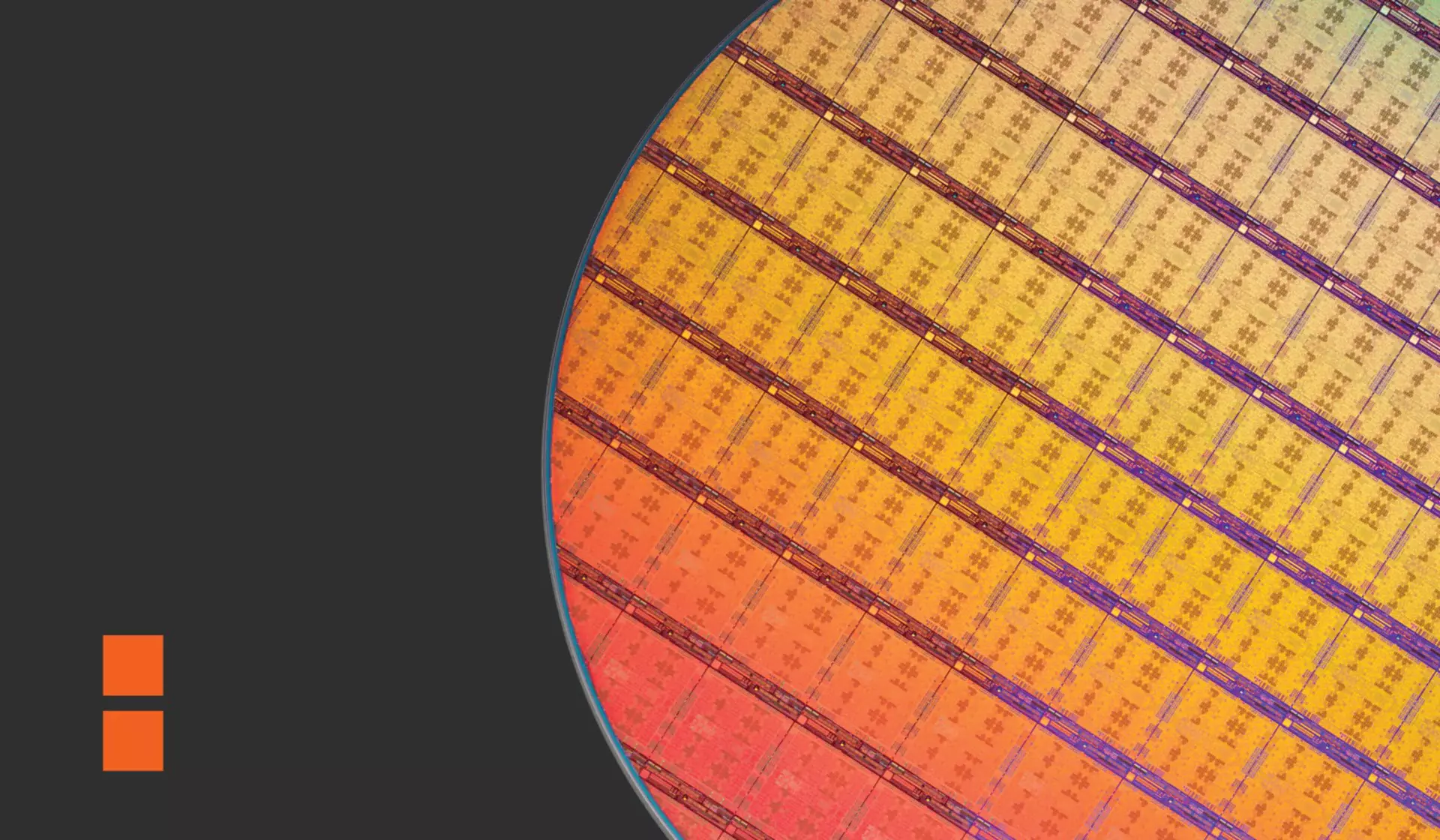
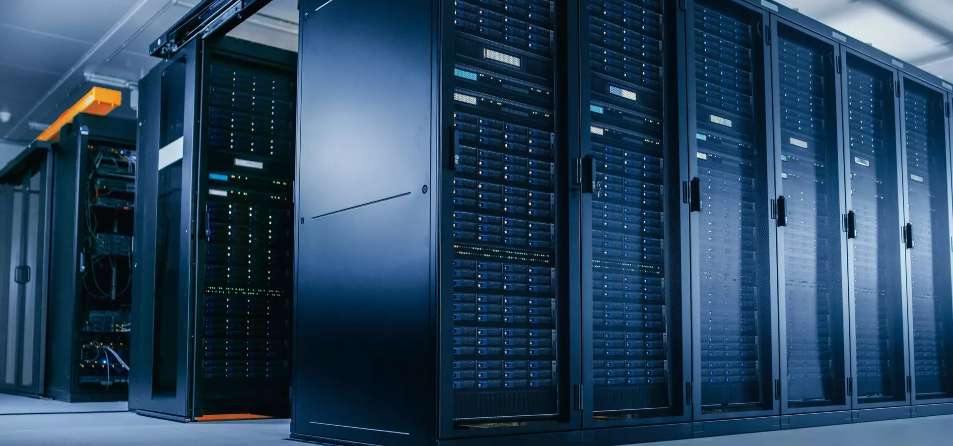
卓越制造,全球与本地并重

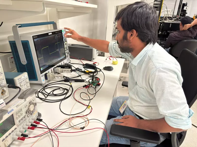
凭借核心技术服务于多元化的市场


最新资讯与前沿观察
-
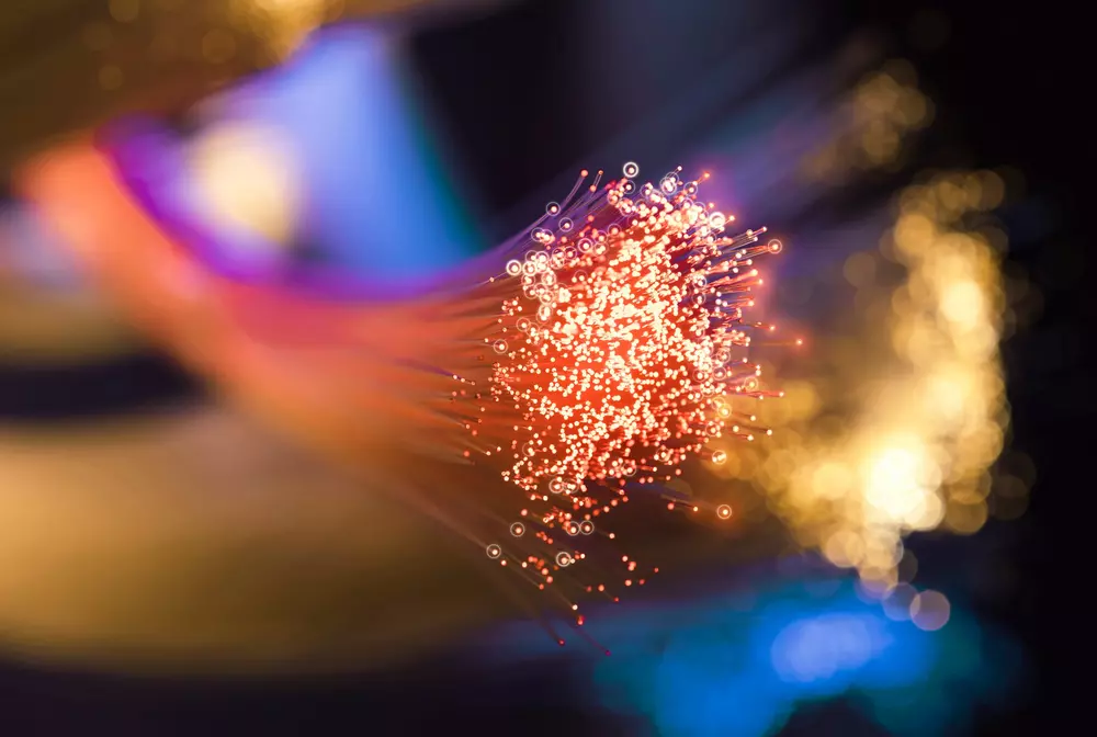
 了解更多:短循环创新:通过端到端设计与验证加速氮化镓(GaN)的应用
短循环创新:通过端到端设计与验证加速氮化镓的应用
-
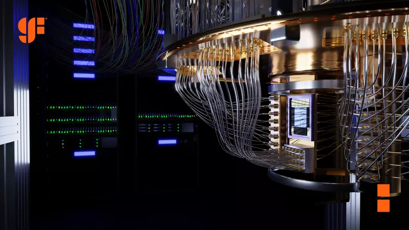
了解更多:SEALSQ 与 GlobalFoundries 合作,共同推动后量子密码学和量子计算技术的发展 (在新标签页中打开)
SEALSQ 与 GlobalFoundries 合作,共同推动后量子密码学和量子计算技术的发展
-
了解更多:MOSIS 2.0 与 GlobalFoundries 的合作:一项旨在推动半导体创新的战略联盟 (在新标签页中打开)
MOSIS 2.0 与 GlobalFoundries 的合作:推动半导体创新的战略联盟
-
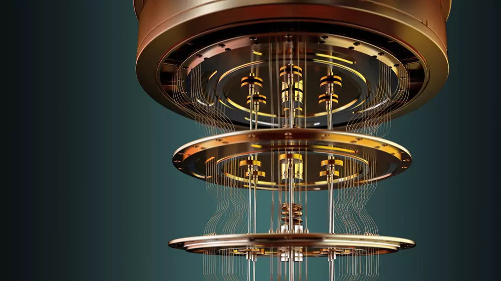
了解更多:量子计算的未来取决于大规模量产
量子计算的未来取决于大规模量产

GF Connect 门户
与GF合作,比以往任何时候都更快速、更轻松地管理您的订单。访问与设计、工程、质量、生产和物流相关的应用程序及信息。
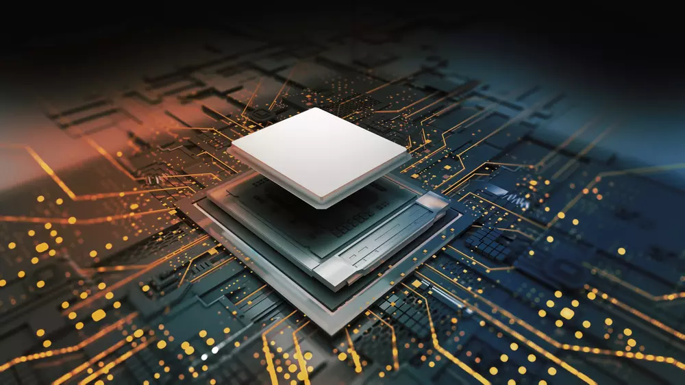
我们塑造重要的东西
关键芯片是现代生活的基石,而我们正是这些芯片的制造者。GF 是一家具备差异化优势的技术合作伙伴,凭借遍布全球的灵活布局,将研发、知识产权、设计、定制芯片与先进制造能力融为一体。依托与客户、政府及生态系统合作伙伴建立的深厚合作关系,我们助力实现最重要的目标。