

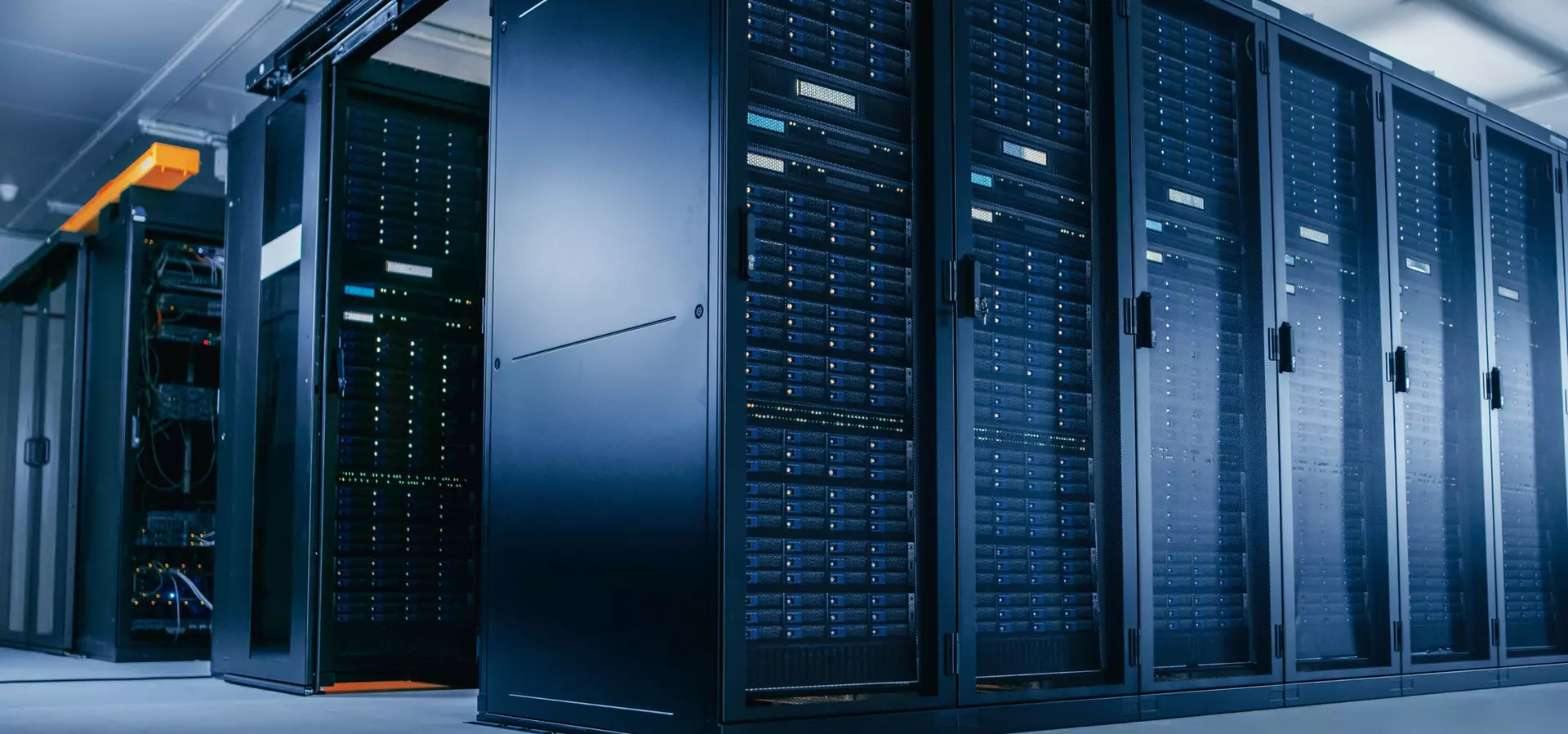
Technologien
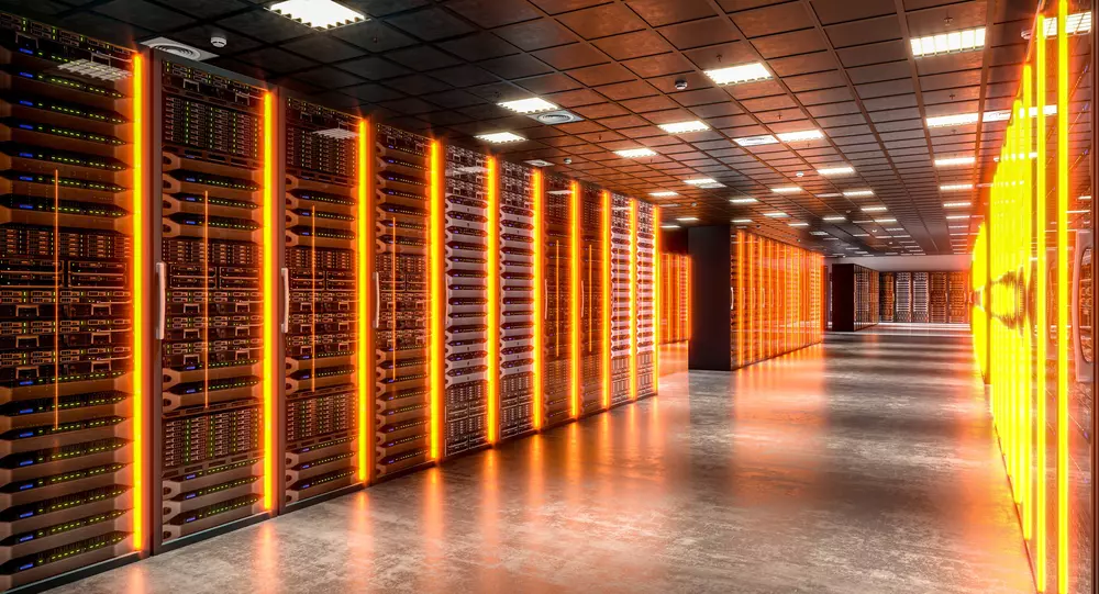


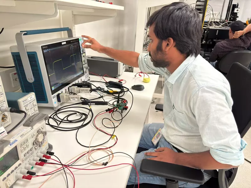
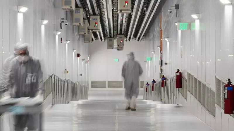
Hervorragende Fertigungsqualität – weltweit und vor Ort

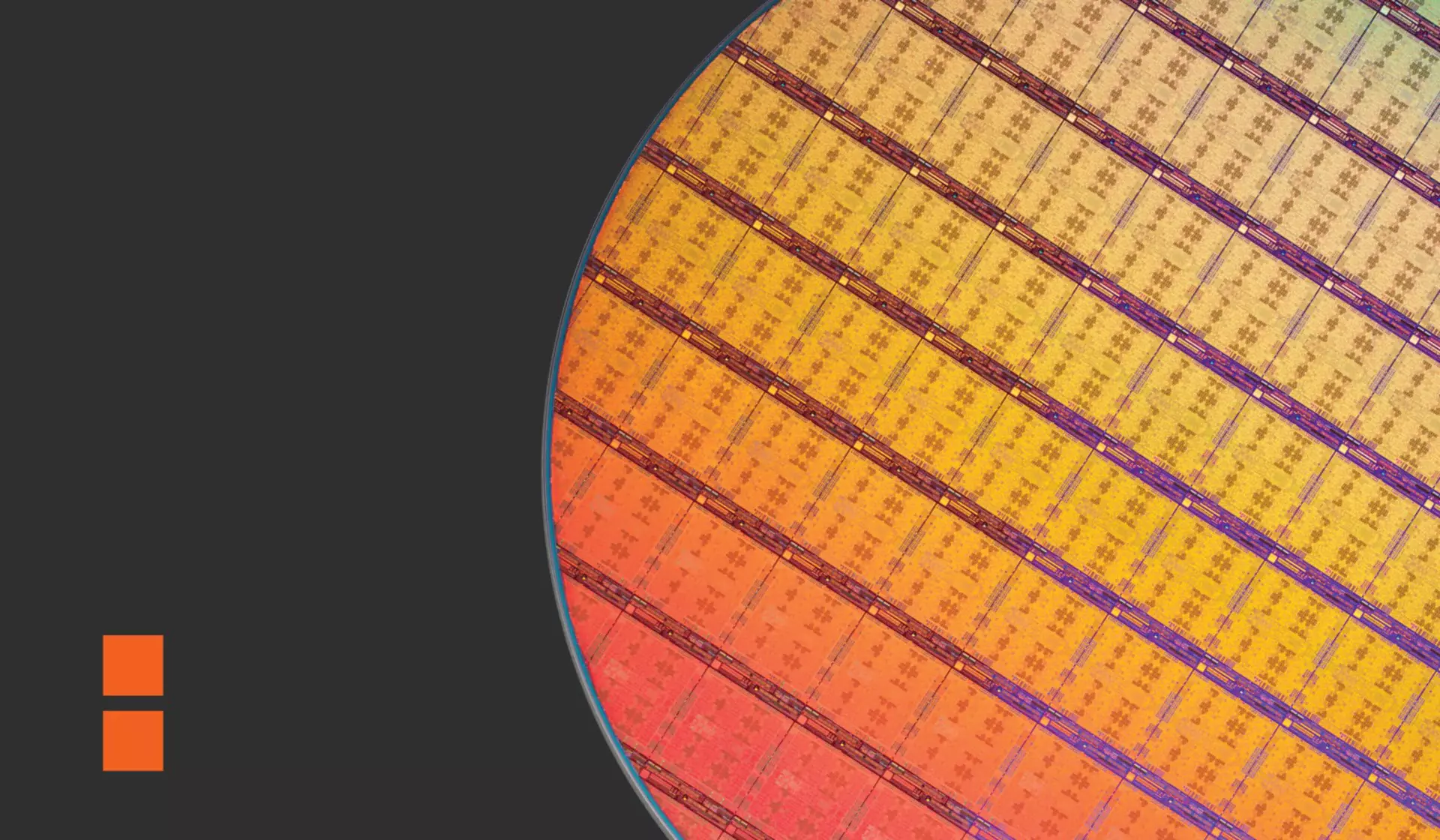
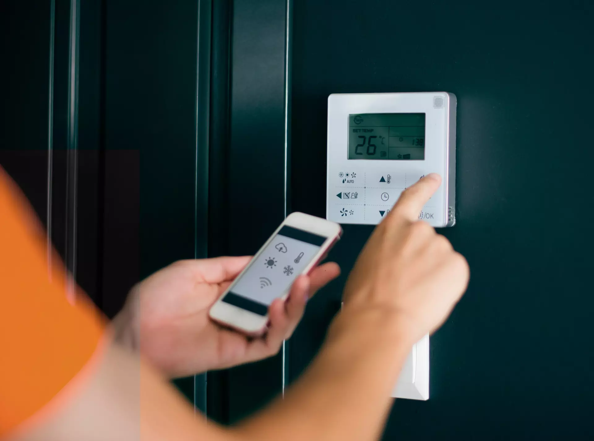
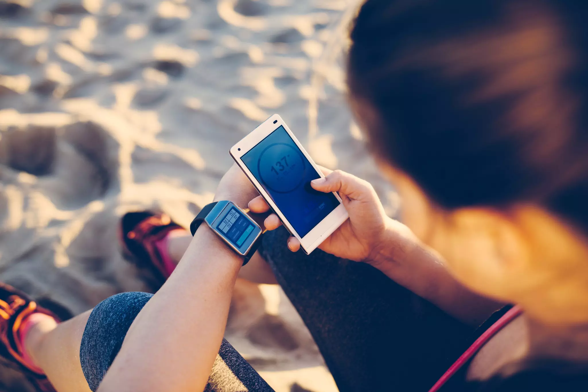
Wir versorgen vielfältige Märkte mit grundlegenden Technologien

Aktuelle Nachrichten & Einblicke
-
 Weitere Informationen: Innovation durch „Short-Looping“: Beschleunigung der GaN-Einführung durch durchgängiges Design und Validierung
Innovation durch kurze Entwicklungszyklen: Beschleunigung der GaN-Einführung durch durchgängiges Design und Validierung
-
Weitere Informationen: SEALSQ und GlobalFoundries schließen Partnerschaft zur Beschleunigung der Entwicklung von Post-Quanten-Kryptografie und Quantencomputing-Technologien (wird in einem neuen Tab geöffnet)
SEALSQ und GlobalFoundries gehen eine Partnerschaft ein, um die Entwicklung von Post-Quanten-Kryptografie und Quantencomputing-Technologien voranzutreiben
-
Weitere Informationen: MOSIS 2.0 und GlobalFoundries – eine strategische Allianz für Innovationen im Halbleiterbereich (wird in einem neuen Tab geöffnet)
MOSIS 2.0 und GlobalFoundries: Eine strategische Allianz für Innovationen im Halbleiterbereich
-
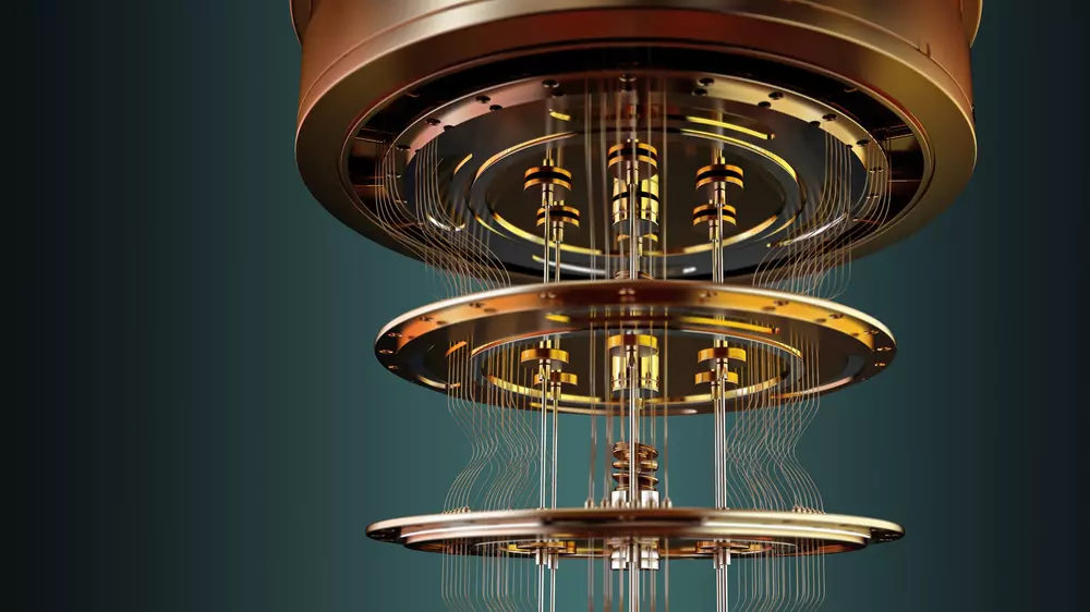
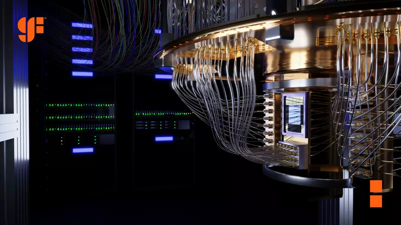
Mehr erfahren: Die Zukunft von Quantum hängt von der Serienfertigung ab
Die Zukunft von Quantum hängt von der Serienfertigung ab

GF Connect-Portal
Arbeiten Sie mit GF zusammen und verwalten Sie Ihre Bestellungen schneller und einfacher als je zuvor. Greifen Sie auf Anwendungen und Informationen aus den Bereichen Design, Technik, Qualität, Produktion und Logistik zu.
Wir gestalten das Wesentliche
Systemchips bilden die Grundlage des modernen Lebens – und wir stellen sie her. GF ist ein einzigartiger Technologiepartner, der Forschung und Entwicklung, geistiges Eigentum, Design, kundenspezifische Halbleiter und fortschrittliche Fertigung in einem flexiblen globalen Netzwerk vereint. Auf der Grundlage enger Partnerschaften mit Kunden, Regierungen und Partnern aus dem Ökosystem ermöglichen wir das, was wirklich zählt.